
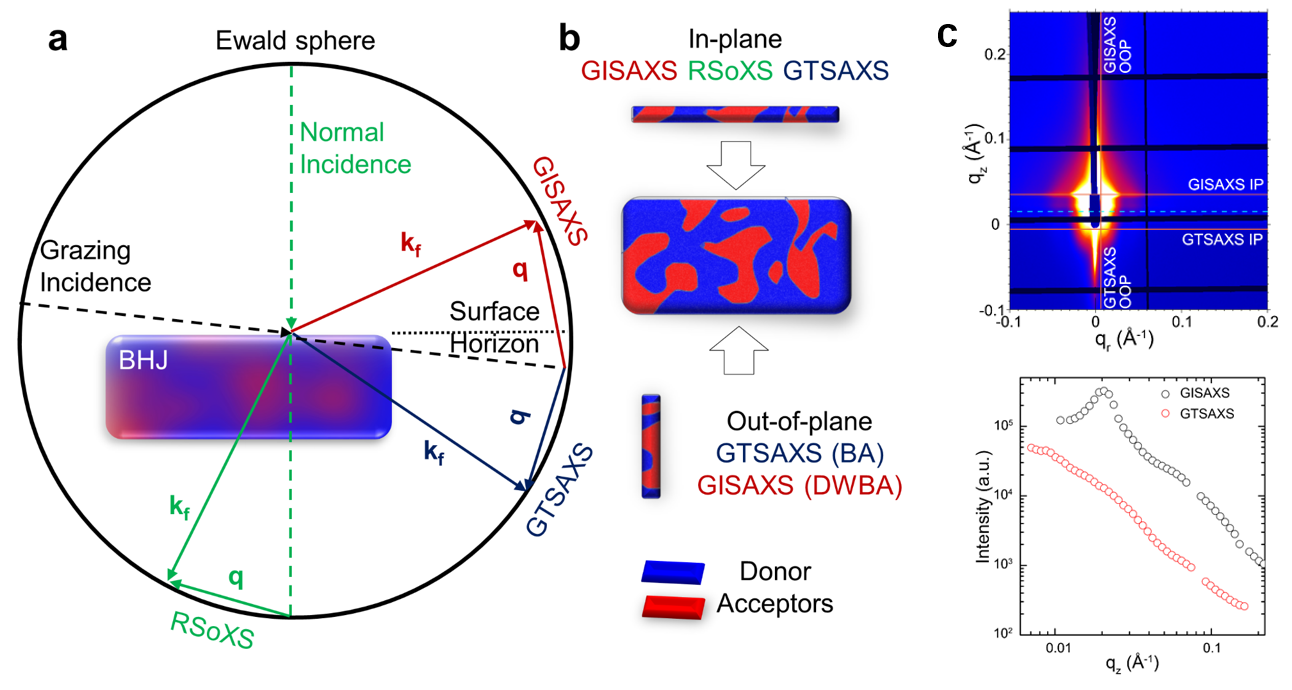
The record power conversion efficiency of organic photovoltaic (OPV) has been boosting rapidly with the development of novel materials and morphology optimization of bulk heterojunction (BHJ) active layer. However, the quantitative determination of out-of-plane nanoscale phase structure of BHJ is still under great challenge. The thin film device structure breaks the symmetry into the in-plane (IP) direction and out-of-plane (OOP) direction with respect to the substrate, leading to an intrinsic anisotropy in the bulk morphology. Due to the charge transport in BHJ active layer is mainly along OOP direction, the quantitative characterization of OOP phase morphology should be of great importance. In this work, we utilized an X-ray scattering technique, Grazing-incident Transmission Small-angle X-ray Scattering (GTSAXS), to uncover this new morphology dimension. The measurement method of GTSAXS on OPV BHJ thin film was formalized systematically. This technique was implemented on the model systems based on fullerene derivative (P3HT:PC71BM) and non-fullerene systems (PBDB-T:ITIC, PM6:Y6), which demonstrated the successful extraction of the quantitative out-of-plane acceptor domain size of OSC systems. The detected IP and OOP domain sizes by GTSAXS show strong correlations with the device performance, particularly in terms of exciton dissociation and charge transfer. Overall, the OOP nanomorphology of OPV BHJ thin film was determined for the first time by GTSAXS, which should be able to provide a new avenue for the future novel photovoltaic materials development and OPV device optimization.
Manuscript by Xia et al. was just accepted by Nature Communications, 2021, 12, 6226, DOI: 10.1038/s41467-021-26510-6.