News Centre
CUHK Develops “Universal Ink” for Direct Laser Writing of High-performance Electronics
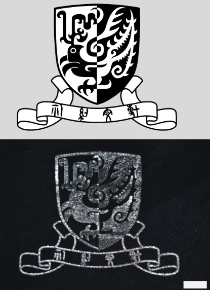
The core of high-performance chip manufacturing is to pattern microscale and nanoscale material structures with high precision. Due to its high-level technical requirements, the production cost remains very high, and the procedures are complex and time consuming. A research team from the Department of Physics at The Chinese University of Hong Kong (CUHK), led by Professor YANG Sen, Assistant Professor, and Dr. XIA Kangwei from the University of Stuttgart, has developed an “universal ink” which can make electronics fabrication as simple as writing Chinese calligraphy. When combined with the single-step laser direct writing technology, high performance chip can be produced with simple equipment and low costs. The research finding has been published in Nature Communications, and CUHK has filed patents for this new technology.
Ideas developed from fundamental physics principles
Photolithography is the most developed chip manufacturing technology and has been widely adopted by the industry for years. The current photolithography technique involves complex procedures that include multiple cycles of spin coating of photoresist, positioning, exposure, developing, evaporation deposition, electroplating and lift-off process, and requires expensive equipment such as mask aligner and a vapour deposition machine, raising the production costs and difficulties. Alternative laser writing techniques, such as those based on nano-metal particle deposition, are limited by the poor electrical properties, mechanical properties and spatial resolutions.
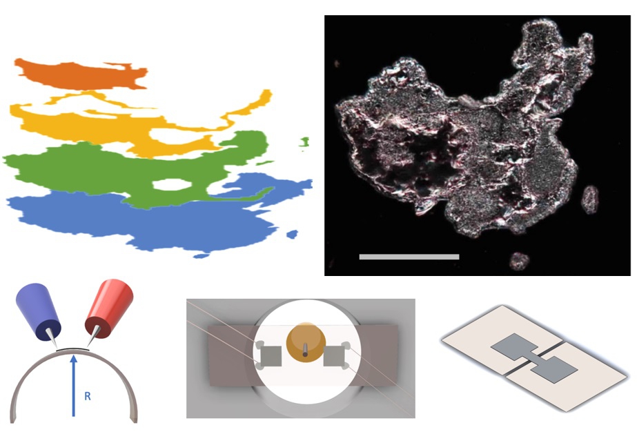
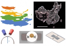
Stemming from fundamental physics principles, the research team came up with a brand-new idea for the material deposition. They combined the optical tweezer technique and semiconductor photoelectric effect, by introducing semiconductor nanoparticles suspension into metallate solution to form the “universal ink”. The focused laser beam triggers both effects simultaneously and induces chemical reduction reaction on the nanoparticles. The reduced metal particles accumulated on the semiconductor nanoparticles work as “glue” to join each other into a solid structure and attach to the substrate. By changing the focus position, selective deposition at an arbitrary position on the substrate is achieved. Through change of “ink” recipes, the team realised deposition with various materials on different substrates.
Using the traditional calligraphy ink for modern micro-nano material fabrication
After searches and trials, the team found that the carbon ink used by traditional Chinese calligraphy and ink painting is one of the best choices as the nanoparticles in this technology. The finished deposition has a performance comparable with the current technologies. It met the criteria for real applications in terms of its nanoscale precision, mechanical flexibility for a flexible device, and excellent conduction and insulation abilities comparable with corresponding bulk material. This technology can be realised with simple equipment and thus, can be easily adapted everywhere. Moreover, the “universal ink” based on carbon ink is environmental-friendly in terms of its low-cost and recyclability.
Unique Application Prospect
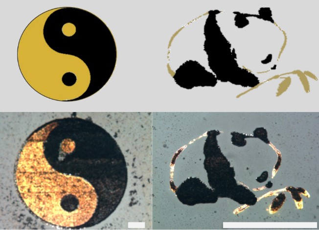
Prof. YANG stated, “The novel single-step laser direct writing technology offers two distinct advantages. First, it can deposit multiple materials with high precision, which enables fabrication of complex images made of different materials. Second, users can integrate an optical detection/measurement device with this laser writing platform to monitor the deposition quality in situ, which will facilitate chip manufacture, especially the quantum computing chip.”
This technology also provides distinct solutions to problems unapproachable by other current technology, such as electrode restoration and fabrication of electronics on a 3D scale. The research team has seen its potential to cover more materials and extend application to a broader field due to the universality of technology mechanism, and they will continue their study and development of this technology for more discoveries.
About the Research Team
Prof. YANG Sen’s group works on experimental quantum information science, including quantum computing, quantum communication and quantum sensing. His group studies quantum optics based on carbon material, particularly the nitrogen vacancy centers in diamond. The group has developed the world’s first highly efficient quantum optics memory based on single nuclear spin in diamond, and quantum sensor for high pressure quantum material research. The group currently focuses on developing diamond-based quantum chips, establishing a remote optical quantum network and studying superconductivity and magnetic properties of quantum materials.
The research team for this work includes Dr. XIA Kangwei, CUHK physics undergraduate student LO Wing Ki, graduate students CHEN Yifan, HUNG Siu Fai, CHEN Yang and SHEN Yang. CHEN Yifan and HUNG Siu Fai are the co-first authors.
Dr. XIA was a Research Assistant Professor at CUHK Physics, and currently works at University of Stuttgart. His research mainly focuses on single rare-earth spectroscopy and carbon-based photochemistry.
The research is funded by CUHK and the Research Grants Council of Hong Kong. During the work, the team received technical support from the Central Lab in the Department of Physics at CUHK.
Reference: https://www.nature.com/articles/s41467-020-19210-0

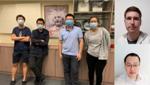
The research team from CUHK Physics discovers that carbon ink used by traditional Chinese calligraphy and ink painting is one of the best choices as the nanoparticles in this technology.
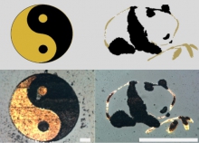
Examples of double metal (platinum and gold) printing. Left: taichi double fish pattern, right: panda. (The scale bar represents 50um.)

